Working with Dr. Dawei Gong,
his postdoctoral research associate, and Prof. Craig Grimes who was
then at Kentucky,
he pioneered growth of TiO2
nanotubes through anodization of pure titanium, a new type of inorganic
oxide nanotubes. As the corresponding
author, Prof. Chen first presented this work at Symposium Z3.9, 2001
MRS Fall
Meeting, Nov. 26-29, 2001, Boston, MA, USA (http://www.mrs.org/f01-program-z/).
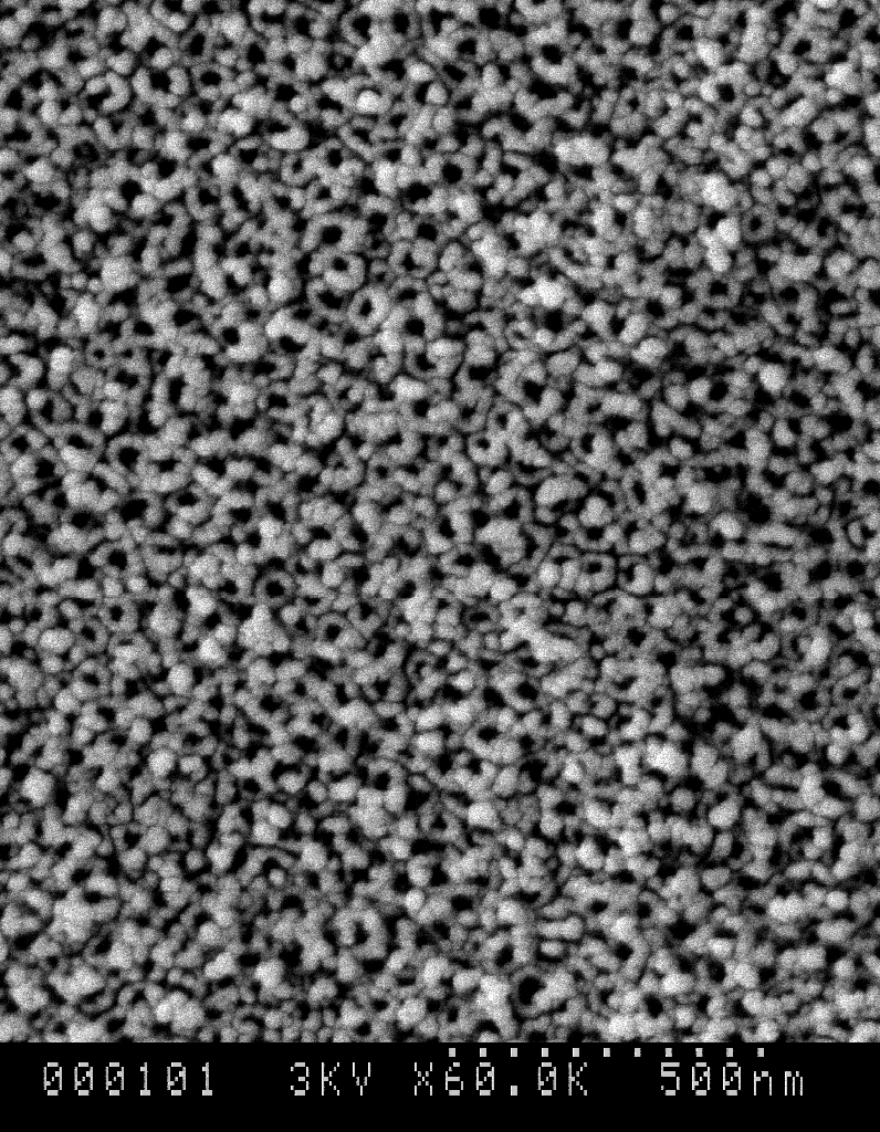
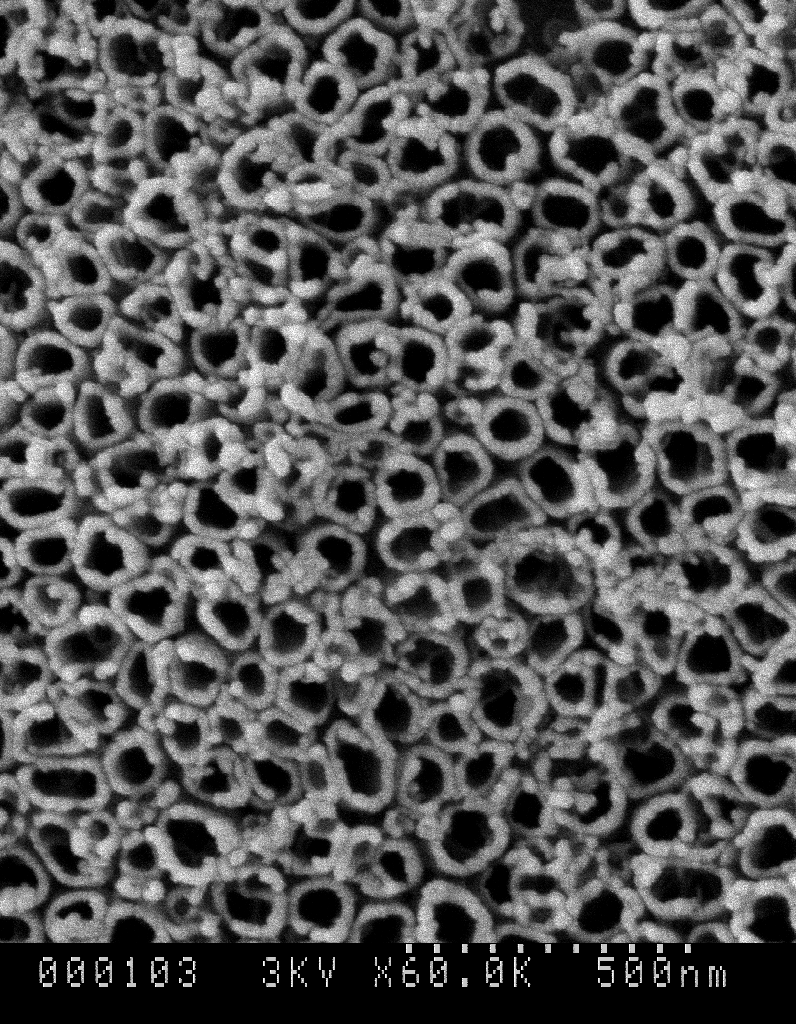
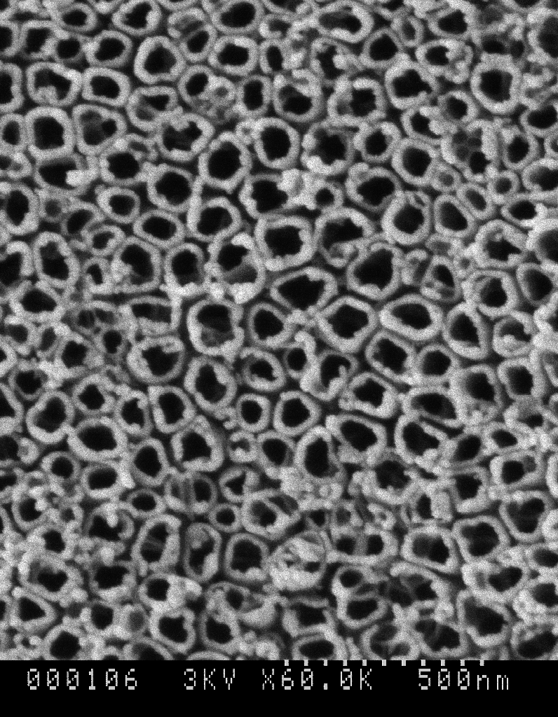
Below are some of the unpublished images in 2001. When the processing
parameters were changed, gradually the TiO2 nantubes showed
up!
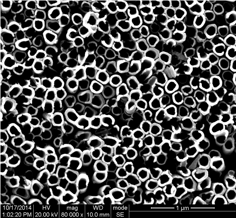
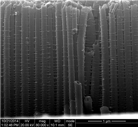
Growth of high-quality TiO2
nanotubes on FTO
Xiaohui
Yang, Xiongbang Wei, Shuanghong Wu, Tao Wu, Zhi Chen, and Shibin
Li, J Mater Sci: Mater Electron (2015) 26:7081–7085
Most high-quality TiO2 nanotube arrays were grown on Ti
foils. The quality of TiO2 nanotubes grown directly on FTO
glasses was very poor without well organization.
We successfully grew of high-quality TiO2 nanotube
arrays
directly on FTO glasses.
|